-

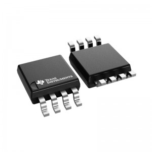
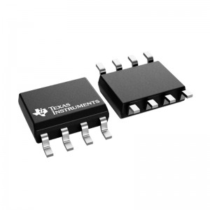
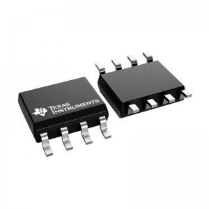
SN75LBC176DR SOP-8 Electronic components integrated circuit transceiver 4.75V-5.25V
SN75LBC176DR Differential Bus Transceiver
The SN55LBC176, SN65LBC176, SN65LBC176Q, and SN75LBC176 differential bus transceivers are monolithic, integrated circuits designed for bidirectional data communication on multipoint bus-transmission lines. They are designed for balanced transmission lines and meet ANSI Standard TIA/EIA-485-A (RS-485) and ISO 8482:1987(E).
The SN55LBC176, SN65LBC176, SN65LBC176Q, and SN75LBC176 combine a 3-state, differential line driver and a differential input line receiver, both of which operate from a single 5-V power supply. The driver and receiver have active-high and active-low enables, respectively, which can externally connect together to function as a direction control. The driver differential outputs and the receiver differential inputs connect internally to form a differential input/output (I/O) bus port that is designed to offer minimum loading to the bus whenever the driver is disabled or VCC = 0. This port features wide positive and negative common-mode voltage ranges, making the device suitable for party-line applications. Very low device supply current can be achieved by disabling the driver and the receiver.
-

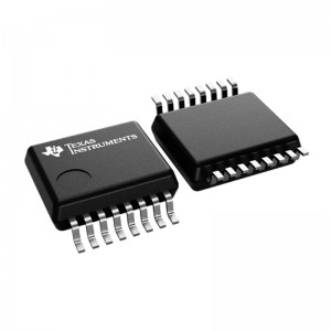
AM26C31IPWR TSSOP-16 Electronic components integrated circuit drive 4.5V-5.5V
AM26C31IPWR
ACTIVE
Quadruple differential line driverThe AM26C31 device is a differential line driver with complementary outputs, designed to meet the requirements of TIAVEIA- 422-B and ITU (formerly CCITT). The 3-state outputs have high-current capability for driving balanced lines, such as twisted -pair or parallel-wire transmission lines, and they provide the high-impedance state in the power-off condition. The enable functions are common to all four drivers and offer the choice of an active-high (G) or active-low (G) enable input BiCMOS circuitry reduces power consumption without sacrificing speed. The AM26C31C device is characterized for operation from 0°C to 70°C, the AM26C311 device is characterized for operation from -40°C to 85°C, the AM26C31Q device is characterized for operation over the automotive temperature range of -40°C to 125°C, and the AM26C31M device is characterized for operation over the full military temperature range of – -55°C to 125°C.
-

TPS61240DRVR SON-6 Electronic components integrated circuit DC-DC switching voltage stabilizer 2.3V-5.5V 3.5MHz
AM26C31IPWR
ACTIVE
Quadruple differential line driverThe AM26C31 device is a differential line driver with complementary outputs, designed to meet the requirements of TIA/EIA-422-B and ITU (formerly CCITT). The 3-state outputs have high-current capability for driving balanced lines, such as twisted-pair or parallel-wire transmission lines, and they provide the high-impedance state in the power-off condition. The enable functions are common to all four drivers and offer the choice of an active-high (G) or active-low (G) enable input. BiCMOS circuitry reduces power consumption without sacrificing speed.
The AM26C31C device is characterized for operation from 0°C to 70°C, the AM26C31I device is characterized for operation from –40°C to 85°C, the AM26C31Q device is characterized for operation over the automotive temperature range of –40°C to 125°C, and the AM26C31M device is characterized for operation over the full military temperature range of –55°C to 125°C.
-

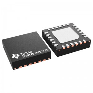
TCA9555RTWR QFN-24 Electronic components integrated circuit 1.65V-5.5V 400kHz
TCA9555RTWR
ACTIVE
16-bit 1.65- to 5.5-V I2C/SMBus I/O expander with interrupt, weak pull-up & config registersThis 16-bit I/O expander for the two-line bidirectional bus(I2C) is designed for 1.65-V to 5.5-V VCCoperation. It provides general-purpose remote I/O expansion for most microcontroller families viathe I2C interface.
The TCA9555 consists of two 8-bit Configuration (input or output selection), Input Port,Output Port, and Polarity Inversion (active high or active low operation) registers. At power on,the I/Os are configured as inputs. The system master can enable the I/Os as either inputs oroutputs by writing to the I/O configuration bits. The data for each input or output is kept in thecorresponding Input or Output register. The polarity of the Input Port register can be invertedwith the Polarity Inversion register.
The TCA9555 is identical to the TCA9535, except for the inclusion of the internalI/O pull-up resistor, which pulls the I/O to a default high when configured as an input andundriven.
Three hardware pins (A0, A1, and A2) are used to program theI2C address, which allows up to eight TCA9555 devices to share the sameI2C bus or SMBus. The fixed I2C address ofthe TCA9555 is the same as the PCF8575,PCF8575C, andPCF8574, allowing up to eight of thesedevices in any combination to share the same I2C bus or SMBus.
-

MAX3232EIDBR SSOP-16 Electronic components integrated circuit transceiver 3V-5.5V
MAX3232EIDBR 3- to 5.5-V dual channel 250kbps RS-232 line driver/receiver with +/-15-kV IEC-ESD protection
The MAX3232E device consists of two line drivers, two-line receivers, and a dual charge-pump circuit with ±15-kV IEC ESD protection pin to pin (serial-port connection pins, including GND).
The device meets the requirements of TIA/EIA-232-F and provides the electrical interface between an asynchronous communication controller and the serial-port connector. The charge pump and four small external capacitors allow operation from a single 3-V to 5.5-V supply. The devices operate at data signaling rates up to 250 kbit/s and a maximum of 30-V/µs driver output slew rate.
-

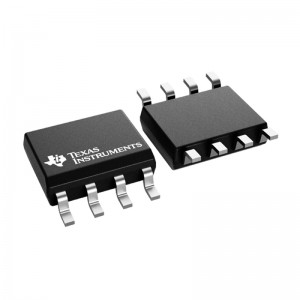
TCAN1042VDRQ1 SOIC-8 Electronic components integrated circuit transceiver
TCAN1042VDRQ1 Automotive fault-protected CAN transceiver with I/O level shifting and flexible data-rate
This CAN transceiver family meets the ISO11898-2 (2016) High Speed CAN (Controller Area Network) physical layer standard. All devices are designed for use in CAN FD networks up to 2 Mbps (megabits per second). Devices with part numbers that include the “G” suffix are designed for data rates up to 5 Mbps, and versions with the “V” have a secondary power supply input for I/O level shifting the input pin thresholds and RXD output level. This family has a low power standby mode with remote wake request feature. Additionally, all devices include many protection features to enhance device and network robustness.
-

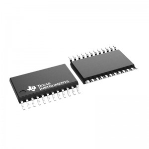
TCA9548APWR TSSOP-24 Electronic components integrated circuit Logic chip 1.65V-5.5V
TCA9548APWR 8-channel 1.65- to 5.5-V I2C/SMBus switch with reset & voltage translation
The TCA9548A device has eight bidirectional translating switches that can be controlledthrough the I2C bus. The SCL/SDA upstream pair fans out to eightdownstream pairs, or channels. Any individual SCn/SDn channel or combination of channels can beselected, determined by the contents of the programmable control register. These downstreamchannels can be used to resolve I2C slave address conflicts. Forexample, if eight identical digital temperature sensors are needed in the application, one sensorcan be connected at each channel: 0-7.
The system master can reset the TCA9548A in the event of a time-out or other improperoperation by asserting a low in the RESET input. Similarly, the power-onreset deselects all channels and initializes the I2C/SMBus statemachine. Asserting RESET causes the same reset and initialization to occurwithout powering down the part. This allows recovery should one of the downstreamI2C buses get stuck in a low state.
The pass gates of the switches are constructed so that the VCC pin can be used to limitthe maximum high voltage, which is passed by the TCA9548A. Limiting the maximum high voltage allowsthe use of different bus voltages on each pair, so that 1.8-V, 2.5-V or 3.3-V parts can communicatewith 5-V parts, without any additional protection. External pullup resistors pull the bus up to thedesired voltage level for each channel. All I/O pins are 5-V tolerant.
-

SN65HVD251DR High Speed CAN Transceiver with Short Loop Delay
SN65HVD251DR
ACTIVE
High Speed CAN Transceiver with Short Loop Delay -

TPD12S521DBTR HDMI transmitter port protection and interface device
TPD12S521DBTR
ACTIVE
HDMI transmitter port protection and interface device -

TPS3808G50DBVR
TPS3808G50DBVR Low-quiescent current supervisor with programmable delay & manual reset
-

TCAN1051HVDR
TCAN1051HVDR
Fault Protected CAN Transceiver With Flexible Data-Rate -

SN65HVD06DR High-Output RS-485 Transceiver
SN65HVD06DR
High-Output RS-485 Transceiver


