Products
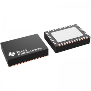
TPS53219ARGTR small-sized single buck controller
Features for the TPS53219A
●Conversion input voltage range: 3 V to 28 V
●VDD input voltage range: 4.5 V to 25 V
●Output voltage range: 0.6 V to 5.5 V
●Wide output load range: 0 A to > 20 A
●Built-in 0.6-V (±0.8%) reference
●Built-in LDO linear voltage regulator
●Auto-skip Eco-Mode™ for light-load efficiency
●D-CAP™ mode with 100-ns load-step response
●Adaptive ON-time control architecture with 8 selectable frequency settings
●4700ppm/°C RDS(on) current sensing
●0.7-ms, 1.4-ms, 2.8-ms and 5.6-ms selectable internal voltage servo soft start
●Pre-charged start-up capability
●Built-in output discharge
●Open-drain power-good output
●Integrated boost switch
●Built-In OVP/UVP/OCP
●Thermal shutdown (non-latch)
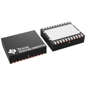
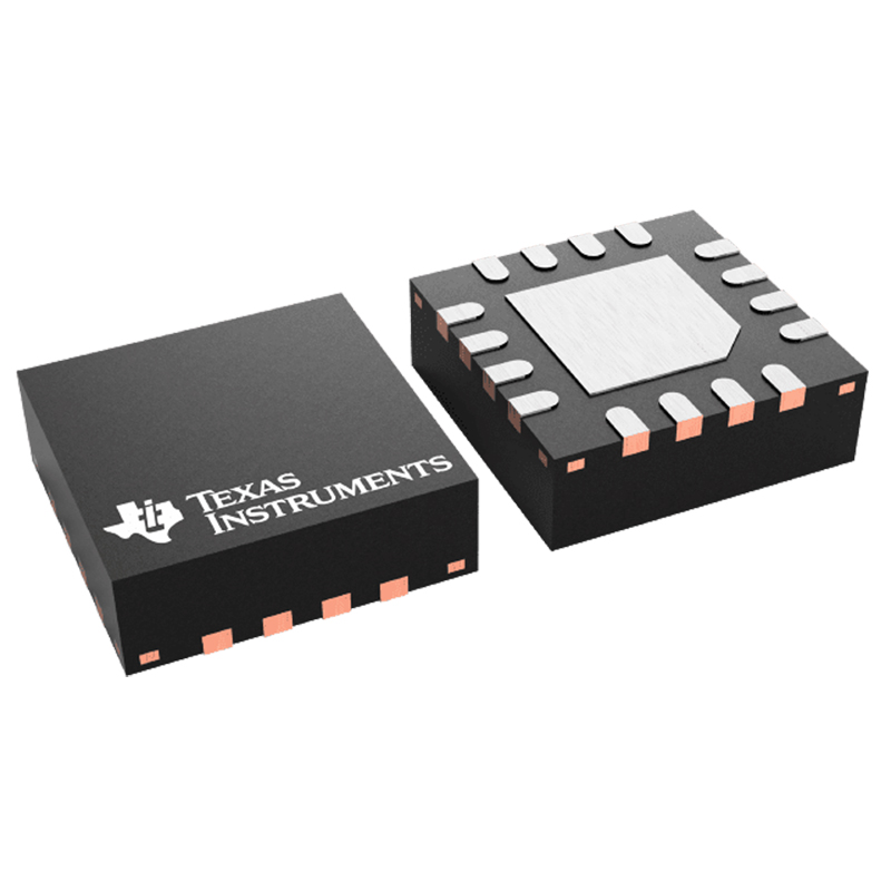
●3-mm × 3-mm QFN, 16-Pin (RGT) package
Description for the TPS53219A
The TPS53219A device is a small-sized single buck controller with adaptive ON-time D-CAPmode control. The device is suitable for low output voltage, high current, PC system power rail andsimilar point-of-load (POL) power supplies in digital consumer products. The small package andminimal pin-count save space on the PCB, while the dedicated EN pin and pre-set frequencyselections simplify the power supply design. The skip mode at light load conditions, strong gatedrivers, and low-side FET RDS(on) current sensing supports low-loss and highefficiency, over a broad load range. The conversion input voltage (high-side FET drain voltage)range is between 4.5 V and 25 V, and the output voltage range is between 0.6 V and 5.5 V. TheTPS53219A is available in a 16-pin, QFN package specified from –40°C to +85°C.
1. Who are the staff in your R & D department? What are your qualifications?
-R & D Director: formulate the company’s long-term R & D plan and grasp the direction of research and development; Guide and supervise r&d department to implement company r&d strategy and annual R&D plan; Control the progress of product development and adjust the plan; Set up excellent product research and development team, audit and training related technical personnel.
R & D Manager: make new product R & D plan and demonstrate the feasibility of the plan; Supervise and manage the progress and quality of r&d work; Research new product development and propose effective solutions according to customer requirements in different fields
R&d staff: collect and sort out key data; Computer programming; Conducting experiments, tests and analyses; Prepare materials and equipment for experiments, tests and analyses; Record measurement data, make calculations and prepare charts; Conduct statistical surveys
2. What is your product research and development idea?
- Product conception and selection product concept and evaluation product definition and project plan design and development product testing and validation launch to market