Products
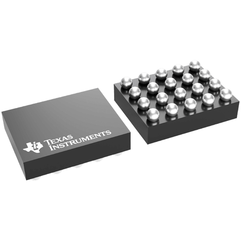
TPS630250YFFR 4-A switch single-inductor buck-boost converter in 3.7 mm² DSBGA package
Features for the TPS630250
Real Buck or Boost Operation with Automatic and
Seamless Transition Between Buck and Boost
Operation
2.3 V to 5.5 V input voltage range
2 A Continuous Output Current : VIN≥ 2.5 V,
VOUT= 3.3 V
Adjustable and Fixed Output Voltage
Efficiency up to 95% in Buck or Boost Mode and
up to 97% when VIN=VOUT
2.5MHz Typical Switching Frequency
35-µA Operating Quiescent Current
Integrated Soft Start
Power Save Mode
True Shutdown Function
Output Capacitor Discharge Function
Over-Temperature Protection and Over-Current
Protection
Wide Capacitance Selection
Small 1.766 mm × 2.086 mm, 20-pin WCSP and
2.5 mm × 3 mm, 14-pin Hot Rod
Description for the TPS630250
The TPS63025x are high efficiency, low quiescent current buck-boost converters suitable for application where the input voltage is higher or lower than the output. Output currents can go as high as 2 A in boost mode and as high as 4 A in buck mode. The maximum average current in the switches is limited to a typical value of 4 A. The TPS63025x regulates the output voltage over the complete input voltage range by automatically switching between buck or boost mode depending on the input voltage ensuring a seamless transition between modes. The buck-boost converter is based on a fixed frequency, pulse-width-modulation (PWM) controller using synchronous rectification to obtain highest efficiency. At low load currents, the converter enters Power Save Mode to maintain high efficiency over the complete load current range. There is a PFM/PWM pin that allows the user to choose between automatic PFM/PWM mode operation and forced PWM operation. During PWM mode a fixed-frequency of typically 2.5 MHz is used. The output voltage is programmable using an external resistor divider, or is fixed internally on the chip. The converter can be disabled to minimize battery drain. During shutdown, the load is disconnected from the battery. The device is packaged in a 20-pin WCSP package measuring 1.766 mm × 2.086mm and 14-pin HotRod package measuring 2.5 mm × 3mm.
1. Who are the staff in your R & D department? What are your qualifications?
-R & D Director: formulate the company’s long-term R & D plan and grasp the direction of research and development; Guide and supervise r&d department to implement company r&d strategy and annual R&D plan; Control the progress of product development and adjust the plan; Set up excellent product research and development team, audit and training related technical personnel.
R & D Manager: make new product R & D plan and demonstrate the feasibility of the plan; Supervise and manage the progress and quality of r&d work; Research new product development and propose effective solutions according to customer requirements in different fields
R&d staff: collect and sort out key data; Computer programming; Conducting experiments, tests and analyses; Prepare materials and equipment for experiments, tests and analyses; Record measurement data, make calculations and prepare charts; Conduct statistical surveys
2. What is your product research and development idea?
- Product conception and selection product concept and evaluation product definition and project plan design and development product testing and validation launch to market


