Products
TUSB212IRWBR 3.6-V, 3-A
Features for the TPS22925
●Input Voltage Range: 0.65 V to 3.6 V
●On-Resistance
○RON = 9.2 mΩ at VIN = 3.6 V
○RON = 9.2 mΩ at VIN = 1.8 V
○RON = 10.2 mΩ at VIN = 1 V
○RON = 13.1 mΩ at VIN = 0.65 V
●3-A Maximum Continuous Switch Current
●Quiescent Current, IQ,VIN = 29 µA at VIN = 3.6 V
●Low Control Input Threshold Enables 1.5-, 1.8-, 2.5-, or 3.3-V Logic
●Controlled Slew Rate
○tR = 97 µs at VIN = 3.6 V (TPS22925Bx)
○tR = 810 µs at VIN = 3.6 V (TPS22925Cx)
●Reverse Current Blocking (When Disabled)
●Quick Output Discharge (QOD) (TPS22925B and TPS22925C only)
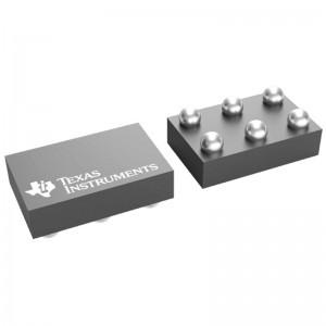
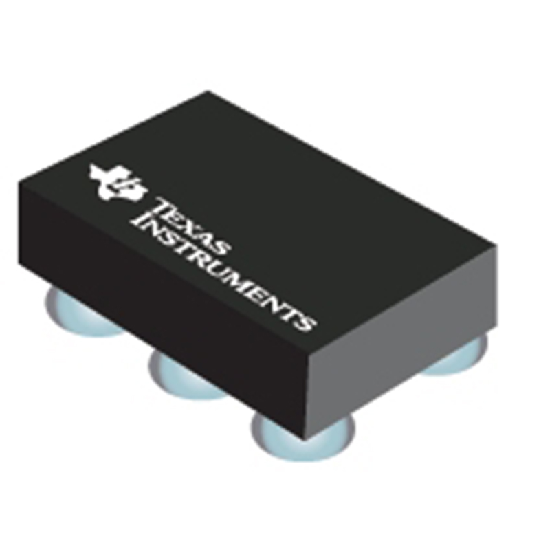
●Wafer Chip Scale Package:
○0.9 mm × 1.4 mm, 0.5-mm Pitch, 0.4-mm Height
●ESD Performance Tested per JESD 22
○2-kV HBM and 1-kV CDM
Description for the TPS22925
The TPS22925 product family consists of four devices: TPS22925B, TPS22925BN, TPS22925C, and TPS22925CN. Each device is a 9-mΩ, single-channel load switch with a controlled slew rate.
The devices contain an N–channel MOSFET that can operate over an input voltage range of 0.65 V to 3.6 V and can support a maximum continuous current of 3 A. This continuous current enables the devices to be used across multiple designs and end equipments. Each of the TPS22925 devices provides reverse current blocking when disabled allowing for power supply protection and power multiplexing capabilities.
The controlled rise time for the device greatly reduces inrush current caused by large bulk load capacitances, thereby reducing or eliminating power supply droop. When operating with an input voltage of 3.6 V, the TPS22925Bx devices feature a 97 µs rise time and the TPS22925Cx devices feature an 810 µs rise time.
The TPS22925 family of devices can help reduce the total solution size by offering an optional integrated, 150-Ω pull–down resistor for quick output discharge (QOD) when the switch is turned off. Each of the TPS22925 devices is available in a 0.9 mm × 1.4 mm, 0.5-mm pitch, 0.4-mm height 6–pin wafer chip scale package (WCSP) allowing for smaller, more integrated designs. The WCSP and 9 mΩ of on-resistance allow use in space constrained, battery powered applications. The device is characterized for operation over the free–air temperature range of –40°C to +105°C.
1. Who are the staff in your R & D department? What are your qualifications?
-R & D Director: formulate the company’s long-term R & D plan and grasp the direction of research and development; Guide and supervise r&d department to implement company r&d strategy and annual R&D plan; Control the progress of product development and adjust the plan; Set up excellent product research and development team, audit and training related technical personnel.
R & D Manager: make new product R & D plan and demonstrate the feasibility of the plan; Supervise and manage the progress and quality of r&d work; Research new product development and propose effective solutions according to customer requirements in different fields
R&d staff: collect and sort out key data; Computer programming; Conducting experiments, tests and analyses; Prepare materials and equipment for experiments, tests and analyses; Record measurement data, make calculations and prepare charts; Conduct statistical surveys
2. What is your product research and development idea?
- Product conception and selection product concept and evaluation product definition and project plan design and development product testing and validation launch to market