Products

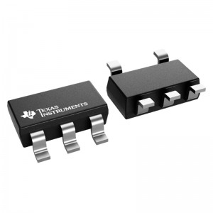
UCC27531DBVR 35-V VDD, and split outputs
Features for the UCC27531
Low-cost gate driver (offering optimal solution for driving FET and IGBTs)
Superior replacement to discrete transistor pair drive (providing easy interface with controller)
TTL and CMOS compatible input logic threshold (independent of supply voltage)
Split output options allow for tuning of turnon and turnoff currents
Inverting and noninverting input configurations
Enable with fixed TTL compatible threshold
High 2.5-A source and 2.5-A or 5-A sink peak drive currents at 18-V VDD
Wide VDD range from 10 V to 35 V
Input and enable pins capable of with standing up to –5-V DC below ground
Output held low when inputs are floating or during VDD UVLO
Fast propagation delays (17-ns Typical)
Fast rise and fall times
(15-ns and 7-ns typical with 1800-pF Load)
Undervoltage lockout (UVLO)
Used as a high-side or low-side driver (if designed with proper bias and signal isolation)
Low-cost, space-saving 5-pin or 6-pin DBV (SOT-23) package options
UCC27536 and UCC27537 pin-to-pin compatible to TPS2828 and TPS2829
Operating temperature range of –40°C to 140°C
Description for the UCC27531
The UCC2753x single-channel, high-speed gate drivers can effectively drive MOSFET andIGBT power switches. Using a design that allows for a source of up to 2.5 A and 5-A sink throughasymmetrical drive (split outputs), coupled with the ability to support a negative turn-off bias,rail-to-rail drive capability, extremely small propagation delay (17 ns typical), the UCC2753xdevices are ideal solutions for MOSFET and IGBT power switches. The UCC2753x family of devices canalso support enable, dual input, and inverting and non-inverting input functionality. The splitoutputs and strong asymmetrical drive boost the devices immunity against parasitic Miller turn-oneffect and can help reduce ground debouncing.
Leaving the input pin open holds the driver output low. The logic behavior of the driveris shown in the application diagram, timing diagram, and input and output logic truth table.
Internal circuitry on VDD pin provides an undervoltage lockout function that holdsoutput low until VDD supply voltage is within operating range.
1. Who are the staff in your R & D department? What are your qualifications?
-R & D Director: formulate the company’s long-term R & D plan and grasp the direction of research and development; Guide and supervise r&d department to implement company r&d strategy and annual R&D plan; Control the progress of product development and adjust the plan; Set up excellent product research and development team, audit and training related technical personnel.
R & D Manager: make new product R & D plan and demonstrate the feasibility of the plan; Supervise and manage the progress and quality of r&d work; Research new product development and propose effective solutions according to customer requirements in different fields
R&d staff: collect and sort out key data; Computer programming; Conducting experiments, tests and analyses; Prepare materials and equipment for experiments, tests and analyses; Record measurement data, make calculations and prepare charts; Conduct statistical surveys
2. What is your product research and development idea?
- Product conception and selection product concept and evaluation product definition and project plan design and development product testing and validation launch to market